 免费发布信息
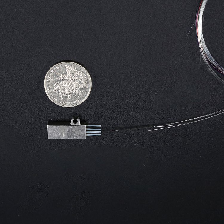
SOI芯片光电探测器 在光通信、物联网及人工智能蓬勃发展的今天,高效、精准的光电转换技术成为支撑智能社会的关键。四川梓冠光电自主研发的SOI(绝缘体上硅)芯片光电探测器,凭借硅基锗-硅工艺的颠覆性创新,正引领着光电探测领域的新潮流。本文将深度解析其技术原理、核心参数、应用潜力及生产制造优势,为您揭示这一“硅基之...
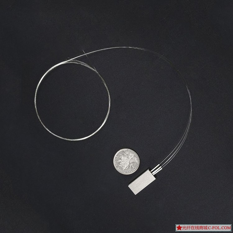
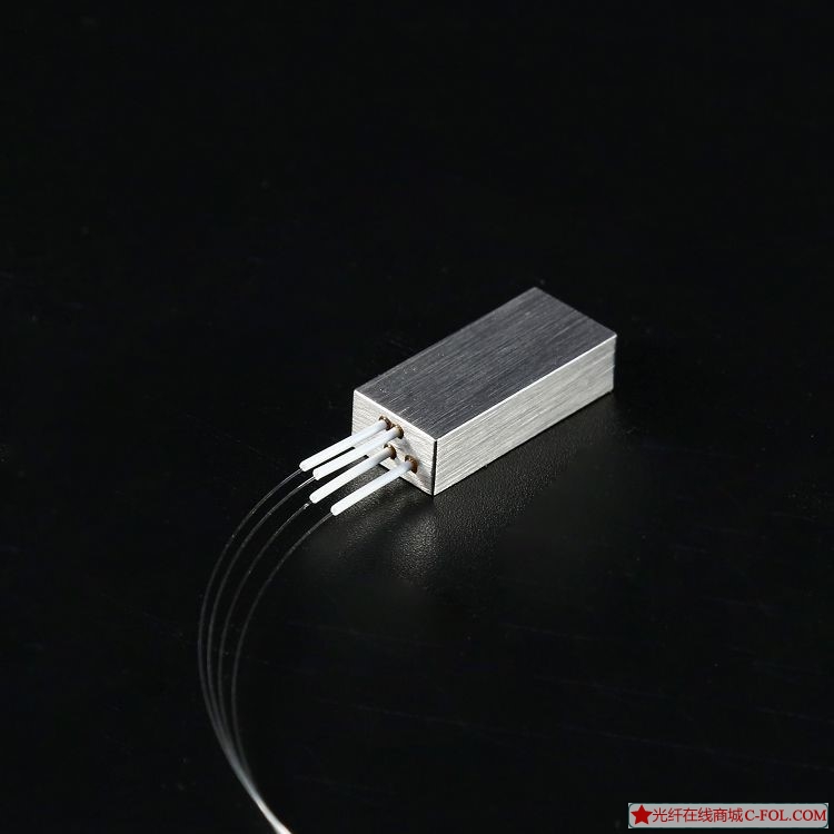
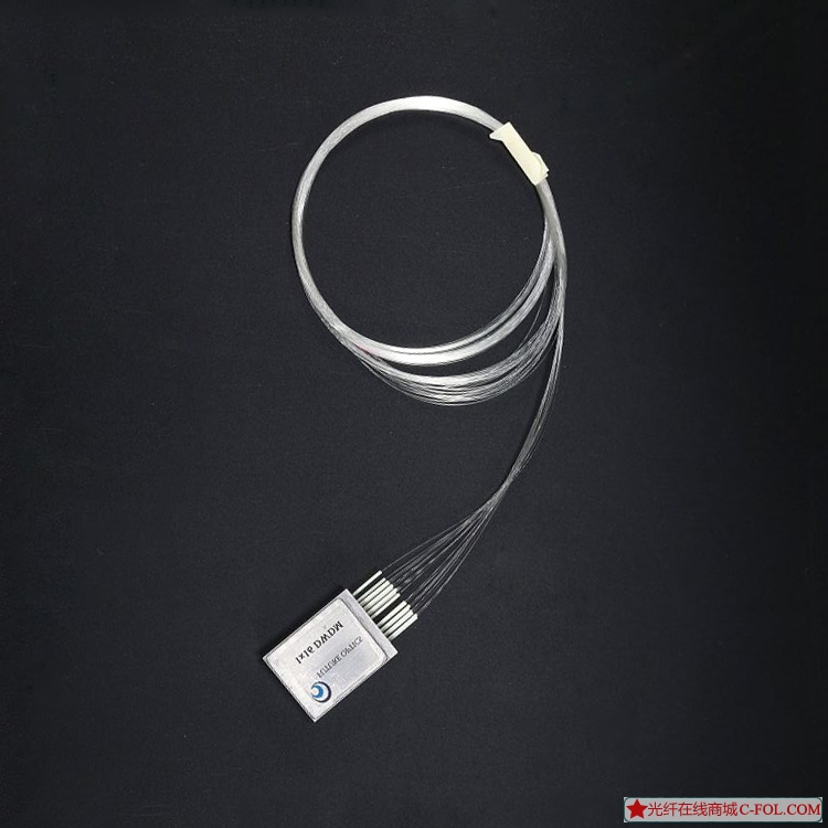
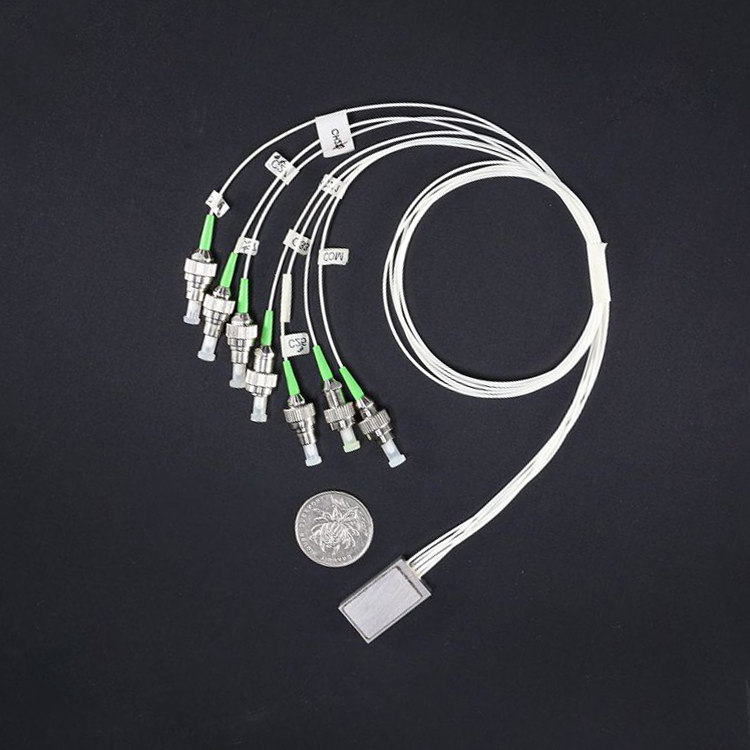
SOI高速光开关阵列芯片 在5G/6G通信、数据中心及人工智能高速发展的今天,光通信技术正成为支撑未来信息社会的核心基石。作为光网络中的“智能交闸”,SOI(绝缘体上硅)高速光开关阵列以其纳秒级响应、高集成度及优异稳定性,成为光传输、交换与传感领域的革命性器件。 本文将以四川梓冠光电的SOI高速光开关阵列为例,深度解析...
top Passband• 波长精度高/High Precision Wavelength• 高可靠性/Highly Reliable and Stable• 符合标准Telcordia GR 1209/1221 Qualified特点/Features• 光路无胶/Epoxy-Free Optical Path• 宽阔平坦的通带/Wide- and Flat-top Passband• 波长精度高/High Precision Wavelength• 高可靠性...
tomization通道间隔/Channel spacingnm20通带宽度/Pass bandwidthnmlc±6.5最大插损/Insertion loss(Max)dB≤1.2典型插损/Insertion loss(Typical)dB≤1.0波长热稳定性/Wavelength thermal stabilitynm/℃≤0.002相邻通道隔离/Adjacent channel isolationdB≥30非相邻通道隔离/No-adjacent channel isolationdB≥40回波损耗/Return lo...

torage temperature°C-40~+85封装尺寸/Footprint dimension (LxWxH)mm21*15.5*6.5 or 21*15.5*5.95尾纤长度/Pigtail lengthm≥1.0 ...
to 1611nm (Except for 1391nm and 1411nm)通道间隔/Channel spacingnm20通带宽度/Pass bandwidthnmlc ± 6.5最大插损/Insertion loss(max)dB≤1.8典型插损/Insertion loss(typical)dB≤1.4波长热稳定性/Wavelength thermal stabilitynm/℃≤0.002相邻通道波长/Adjacent channel isolationdB≥30非相邻通道波长/No-adjacent channel i...
torage temperature°C-40~+85封装尺寸/Footprint dimension (LxWxH)mm21*15.5*6.5 or 23*15.5*5.9尾纤长度/Pigtail lengthm≥1.0...
torage temperature°C-40~+85封装尺寸/Footprint dimension (LxWxH)mm20*12*6.5 or 20*12*5.95尾纤长度/Pigtail lengthm≥1.0...
torage temperature°C-40~+85封装尺寸/Footprint dimension (LxWxH)mm20*12*6.5 or 20*12*5.95尾纤长度/Pigtail lengthm≥1.0...

torage temperature°C-40~+85封装尺寸/Footprint dimension (LxWxH)mm21*15.5*6.5 or 21*15.5*5.95尾纤长度/Pigtail lengthm≥1.0 ...
 |
|